Laser Wafer Dicing – A Brief History of the Process
4 min read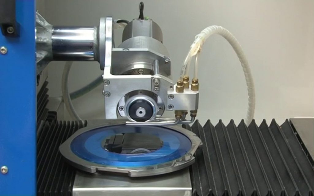
Lasers have allowed many technological breakthroughs in various fields, but the need for wafer-dicing processes has also increased, especially since wafers become more compact. Companies are now replacing their older, conventional thermal cooling systems with laser-based technology and are taking full advantage of the low-feed rate and non-contact system without chipping. With the ever-increasingly tight cost of materials and labor, companies need every tool at their disposal to reduce costs and improve efficiency. This is why companies are looking to lasers for all types of dicing.
Another benefit to using laser wafer dicing is that it reduces the risk of surface cracks. Anytime a laser beam is directed at a material, the potential for energy generation is always present. However, when a laser beam strikes a quartz crystal or other smooth flat surface, there is little to no generation of energy. This means that lasers used for dicing can be precisely controlled to cut materials without exposing them to high levels of energy. Since laser beams are so precise, they require very little cleaning after the process is completed. This means that companies will see fewer instances where small pieces of equipment or machinery are accidentally damaged by the high-energy beams.
In addition to reducing the risk of surface damage, laser wafer dicing cuts cost. With less time spent on downtime, companies will find that they can save a significant amount of money on materials and labor costs by opting for this process instead of traditional methods. Standard die-cutting methods, such as sanding, can take up to an hour on a single piece of equipment, but using a laser wafer-dicing machine, the time spent is only a fraction of a second.
Since the lasers used in wafer-dicing technology are capable of cutting through even thick materials, companies stand to save even more money when they implement the process on their own. For example, wafers can be produced on a large scale by using a thin metal plate. However, it takes up to 10 times as long to cut the metal from a single sheet as compared to using a wafer-dicing machine. Instead, many companies choose to purchase a die-cutting machine that can produce the needed wafers per hour.
With today’s semiconductor laser wafer dicing machines, it is possible to reduce the amount of time necessary for the process to be effective. One option is to place the wafer into a vacuum chamber. This method prevents air from entering the semiconductor beams, which reduces the amount of heat generated during the process. By reducing the amount of heat generated in the chamber, companies save both energy and money. In addition, because the laser beam is not exposed to oxygen, no harmful gases are created. In short, using a chamber instead of a vacuum increases the chances of the beam staying intact.
To reduce the amount of time needed for the laser wafer dicing process to work, companies can also increase the thickness of the wafer. The thickness is dependent upon several factors, including the amount of material to be used and the size of the cavity. However, companies must keep in mind that thinning the beam will result in a correspondingly lower output. For this reason, some companies opt for a thicker laser wafer-dishing chamber in order to maintain better results at a reduced cost.
Because of these benefits, many companies have been exploring the use of laser wafer dicing technology for years. While the technology has been available for decades, only recently have scientists found a way to make the process much easier to control. This discovery enabled scientists to successfully create micro-thin silicon wafers. In fact, they succeeded because they were able to fine tune the processes in order to create a micro-thin, uniform wafers. By taking this one small step, companies are paving the way toward creating more durable, more resilient materials. This will ultimately benefit consumers, who will no doubt be impressed with the new materials’ durability.
Although the benefits of laser wafer dicing have been heralded throughout the scientific community, one drawback is that it takes a long time to create perfect results. It can take up to three weeks to perfect one micro-chip. Even though this is a long process, companies still continue to use the technology because they believe it will be of great benefit to their industry. The increased precision and accuracy that these materials offer will make it easier than ever for companies to deliver on their promises.